|
|
|
|
|
|
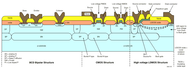
1998-06-25, BG9802, Consumers are increasingly aware of the environment and demanding energy efficient equipment. To address this, equipment manufacturers have to use an IC with energy saving algorithms on it: the problem is that normal CMOS ICs cannot handle mains voltages directly. Philips Semiconductors' solution is to use a process that combines intelligence from digital circuitry with the ability to handle high voltages up to 750V. Called BCD PowerLogic™, it gets its name from the combination of Bipolar, CMOS and DMOS - all on the same chip. This process is the key to the new GreenChip™ range of Switched Power Mode Supplies that the company has just launched. The demand for this technology has been rapidly increasing over the past couple of years at a rate of some 40% per annum, in response to the need for intelligent, power management to save energy. Uses include battery management for power plugs, shavers, mobile phones, and other mains recharging applications, as well as millions of units a year for lighting control in fluorescent lamps and for use in automotive applications. The most important part of the process is the design of the DMOS (Double diffused MOS) parts that handle the high voltage. Philips invented the DMOS structure based on the 'Reduced Surface Field (RESURF)' principle in 1979*, and have been perfecting it ever since. It is the most critical part of the design as it must be able to handle the high voltages, which it does by having a long path (drift region) between the Drain and the Source that attenuates the high voltage down to around 20V. See figure 1. Normally with ICs, the designs can be shrunk to make them smaller but, in this case, shrinking the design would mean that this path reduces and so the voltage attenuation would be smaller. To counteract this, the diffusion profiles of the design have to be carefully optimised to ensure proper voltage attenuation while still realising minimum on-resistance and thus die area. Furthermore, in most applications, the products operate simultaneously at high voltages, high temperatures and high currents. As a result, these technologies must be able to meet stringent reliability requirements. Once the critical DMOS design is done, the design of the CMOS and Bipolar parts is straightforward as these generally use all the same mask stages and can be optimised for maximum performance and minimum area.
Variety of structures
Three main processes
Fine-tuning Philips Semiconductors, a division of Philips Electronics NV, headquartered in Eindhoven, The Netherlands, is the ninth largest semiconductor supplier in the world and the third largest supplier of discretes in the world. Philips Semiconductors' innovations in digital audio, video, and mobile technology position the company as a leader in the consumer, multimedia and wireless communications markets. Sales offices are located in all major markets around the world and are supported by systems labs.
|
|
Copyright © 2000 Royal Philips Electronics All rights reserved. Terms and conditions. |
|