|
|
|
|
|
|
1998-09-21, BG9803,
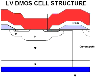
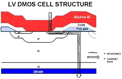
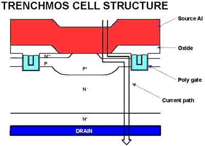
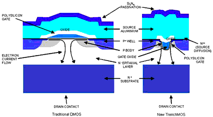
The TrenchMOS process Low resistances are very important for these devices as it means that less waste heat is produced when current passes through them (from the formula current squared times the resistance equals the heat generated). This offers designers a choice of lower heat dissipation for the same sized chip, a higher current handling capability from the same sized chip or a smaller chip with the same dissipation - options that are particularly useful when designing mobile electronic equipment. TrenchMOS products are now being used in almost every part of the electronics industry including automotive, mobile communications, computers and EDP (Electronic Data Processing). "Because we can draw on our extensive CMOS process knowledge, we have been able to use this in PowerFab 2 to enable us to create TrenchMOS structures that are much smaller. The cell pitch (or repeat pattern distance) shrinks from 11 micron to 9 micron, enabling the cell packing density to be increased from 6.2 to 9 million cells per square inch. This ensures that we maintain our leading position in this technology both in terms of price and advanced performance. Because TrenchMOS does not suffer from the so-called JFET effect* that hinders the shrinking of the traditional DMOS structure, we will be able to continue to shrink and refine the TrenchMOS process to achieve even lower resistances over the next few years." * JFET effect. In CMOS, shrinking the feature size means that the chips run at smaller voltages and currents. However, power semiconductors still have to handle the same high voltages and currents, and so shrinking in this case creates a problem not a benefit.
Hexagonal cell structure The new production facilities of PowerFab 2 will enable the cell pitch (or repeat pattern distance) to be shrunk from 11 micron to 9 micron, enabling the cell packing density to be increased from 6.2 to 9 million cells per square inch. This gives a 20% reduction in the Rds(on) so that devices can be made smaller for the same current handling capability, remain the same size but with increased current handling capability, or the same sized device can handle the same current but with less heat dissipation. Products based on this improved TrenchMOS process will start to be phased in later this year. Why is a low resistance so important? When operating at high currents, such as the 50 Amps often found in a car, the heat generated as waste by a solid state switch is proportional to the square of the current times the resistance (i.e. I²R). It is therefore vital to keep the resistance as low as possible otherwise the device will overheat and fail. The new products from Philips Semiconductors have a maximum Rds(on) of 7 milliOhm and will have real life value of around 5.5 milliOhm, with a tolerance of being able to handle a voltage as high as 55V without breaking down. For 25V, the best device in TO220 can have a maximum Rds(on) specification of 5milliOhm with expected real life values of around 3.5 milliOhm.
TrenchMOS products are surface mountable
In demand throughout the electronics industry
|
|
Copyright © 2000 Royal Philips Electronics All rights reserved. Terms and conditions. |
|