|
|
|
|
|
|
1999-04-06, BG9901, Philips Semiconductors, the largest European semiconductor company, has announced details of EZ-HV™ - a brand new process technology for the production of commercial high-voltage silicon-on-insulator (HV-SOI) ICs. The process, which allows ICs to include high-voltage circuits that can handle rectified AC line supply voltages, as well as low-voltage CMOS logic to provide on-chip intelligence, is based on a thin silicon approach to HV-SOI construction that is so novel the company has been awarded a number of patents on it. Until now, such ICs either required the use of a thick layer of silicon to achieve the high breakdown voltage or the use of high-cost substrate materials such as sapphire, both of which made them expensive to produce. "EZ-HV's unique combination of thin silicon and oxide isolation will allow us to integrate virtually any type of circuit element onto an IC alongside 650-volt power transistors," said Leo Warmerdam, Philips Semiconductors' Power Management ICs Marketing Manager. "This makes it possible, for the first time, to produce a whole new generation of single-chip system-on-silicon solutions that include on-chip power handling capabilities." "Combined with Philips Semiconductors' extensive systems-level knowledge in the areas of power management and power conversion, the availability of a commercial process for implementing highly integrated cost-effective solutions opens a whole new world of possibilities for design engineers," he added.
Thinking thin provides breakthrough The conventional way to handle high voltages on an IC is to have a thick layer of silicon overlaying an insulating material - usually silicon dioxide. Although this thick layer of silicon is expensive to produce and difficult to dope, its purpose is to limit the electric field strength in the layer to less than 15 V/mm. If the field strength exceeds 15 V/mm, free charge carriers in the silicon (electrons and holes) may be accelerated by the electric field to the point where they have sufficient energy to generate new electron/hole pairs by impact ionization (collision with atoms in the silicon lattice) - see Figure 1. These new electrons and holes are similarly accelerated by the electric field to energy levels that cause impact ionization, resulting in the generation of even more electron/hole pairs. This regenerative effect, which is termed 'avalanche breakdown', results in so many charge carriers being generated in the silicon that excessive current can flow in the device, permanently damaging it.
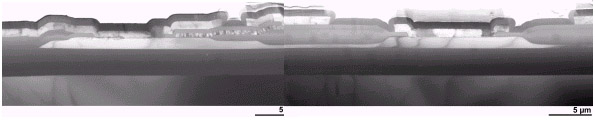
Rather than using this thick-silicon approach to handling high voltages on ICs, the Briarcliff division of Philips' world-renowned research laboratories in New York took an entirely fresh look at the problem. If a thick layer of silicon allows charge carriers to be accelerated over distances that result in them acquiring high enough energy levels to cause avalanche breakdown, why not make the silicon layer so thin that they simply can't move far enough to acquire these energy levels? It was from this highly innovative idea that Philips Semiconductors' new EZ-HV silicon-on-insulator process was born. Instead of the 10 to 20 micron thick layer used in conventional high-voltage silicon-on-insulator processes, the EZ-HV process uses a layer of silicon only half a micron thick (about 1000 atoms), which is much cheaper to produce. Although with 650 volts applied across this layer the vertical field strength is extremely high (1300 V/µm) there is still insufficient distance between the upper and lower layers of the silicon for charge carriers to be accelerated to avalanche breakdown energy levels. Making the layer even thinner starts to present a problem, in that there are fewer charge carriers available to carry the required device current, so a compromise trade-off is reached at half a micron. As well as being cheaper to produce, EZ-HV's 0.5 micron thick silicon layer has other advantages. Because it is so thin, it is easy to locally oxidize the layer in order to create silicon dioxide walls around individual transistors and components - see the far left and far right side of Figure 2. Because silicon dioxide is a perfect insulator, this technique allows high voltage components to be packed very close together, or alongside low-voltage circuitry, while maintaining near perfect isolation between them. In the thick layer approach the layer is too thick to oxidize without first etching deep trenches into it, which because it adds difficult masking and etching steps to the process, increases cost and reduces yield.
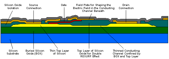
Figure 2 - Cross Section of EZ-HV LDMOS Structure Figure 2 above illustrates the typical structure of a high-voltage LDMOS (Lateral Double-diffused MOS) transistor fabricated using the EZ-HV process. Producing this critical high-voltage component requires the use of only 13 mask steps that fit closely into Philips Semiconductors' standard BiCMOS process flow, making the production of basic EZ-HV ICs cost-effective even for price sensitive applications. However, modular extensions can be added to the process to create a wide range of other components, including high-voltage PMOS transistors, high-voltage LIGBTs (Lateral Insulated-Gate Bipolar Transistors), npn and pnp bipolar transistors, NMOS and PMOS FETS (to create CMOS logic), zener diodes, and passive components such as resistors and capacitors. All these active and passive devices are optimised for fabrication in a bonded silicon-on-insulator layer ranging in thickness between 0.5 and 1.5 microns that sits on a buried oxide layer of 2 to 3 micron thickness. Double layer metal can be added to create a combined double-polysilicon, double-metal process that is useful for co-optimisation of DMOS and CMOS logic, while the double metal option combined with thin-film dielectric isolation provides for extremely dense circuit layout capabilities.
EZ-HV silicon-on-insulator versus bulk silicon In addition to comparing EZ-HV with thick-layer SOI processes, over which it has both cost and integration density advantages, it is also useful to compare it to bulk silicon processes. The most important advantage of EZ-HV over bulk silicon is its oxide isolation, which because it totally surrounds each component with an insulating layer of silicon dioxide reduces parasitic capacitances, eliminates leakage currents, permits integration of a very wide range of active devices and allows high packing densities. In contrast, the junction isolation (reverse biased pn junction) used in bulk silicon ICs precludes the integration of devices such as forward biased diodes and minority carrier injection devices, introduces significant parasitic capacitance and cannot prevent leakage currents from flowing. As a result, bulk silicon solutions for high-voltage power control applications inevitably have to employ separate ICs or a Multi-Chip Module approach, making them bulky and expensive. Using EZ-HV, all the requisite electronics can be created on a single chip to form System-On-Silicon (SOS) solutions that are small, light, inexpensive and easy to design.
Latch up immunity and high operating temperature suit harsh environment applications Compared to bulk silicon processes, Philips Semiconductors' EZ-HV process also has the advantage of being immune to latch-up problems. In bulk silicon ICs, the junction isolation results in the creation of pnpn structures between adjacent transistors. These pnpn structures can act like thyristors, with the potential to be triggered into conduction by the inadvertent injection of holes into the central p region or electrons into the central n region. The most likely cause of triggering is a voltage spike on one of the IC's supply rails, and the resulting current that flows can permanently damage the device. Such spikes are commonplace in electrically noisy power switching applications. Latch up becomes more of a problem as the process geometry shrinks because the sensitivity of the pnpn structures to triggering increases. The EZ-HV process, however, results in ICs that are immune to latch up because not only are there no pnpn junctions between devices, the oxide isolation also ensures that there are no leakage currents. The ability to fabricate several different power components on a single chip without any danger of introducing latch-up problems is a key factor in Philips Semiconductors' ability to create a whole new generation of integrated power control chips using the EZ-HV process. Breakdown of junction isolation in bulk silicon devices, either in the form of excessive leakage current or latch-up, can also be caused by thermally generated charge carriers if the temperature of the device increases to between 125°C and 150°C. However, because of EZ-HV's oxide isolation and latch-up immunity, it will be possible to engineer the EZ-HV process to produce devices that can operate at temperatures well in excess of these figures for special applications such as automotive and aerospace systems.
Reduced parasitic capacitance enables high-frequency switching The significant reduction in parasitic capacitance achieved by using oxide isolation instead of junction isolation enables high-voltage transistors in EZ-HV ICs to switch much faster than those in bulk silicon devices. Faster switching is not only the result of reduced feedback capacitance. The reverse biased isolation junction surrounding a bulk silicon transistor requires a large depletion zone to withstand voltages as high as 650 V, yet the instantaneous width of the depletion zone is determined by the applied voltage. When the transistor is on, the voltage across the junction is very low and the depletion layer is therefore thin. When the transistor turns off, the voltage across the junction increases to the supply voltage and the depletion zone builds up to maximum thickness. The movement of charge carriers into and out of the depletion zone to increase or reduce its thickness each time the transistor turns off or on represents a current through the IC, which heats up because it has significant body resistance. This current flow can also result in localised changes in body potential that cause the IC to malfunction. In practice this limits the switching frequency of high-voltage transistors in bulk silicon ICs to around 100 kHz. By comparison, high-voltage transistors in EZ-HV ICs suffer none of these problems, and can therefore be used at switching frequencies into the MHz range.
Double RESURF effect halves on-resistance EZ-HV transistors can also handle higher currents than the epitaxial transistors used in bulk silicon ICs because the EZ-HV process allows transistors to be fabricated with on-resistance (RDS(on)) values that are half that achievable by any other IC technology. The key area where resistance is critical is in the drift region of the MOSFET, which is there to limit the lateral field strength when the transistor is off (i.e. when there is maximum applied voltage across the device) to a value that is below the avalanche breakdown threshold of the epitaxial silicon. To maximise the high voltage capability of the transistor the drift region should ideally be either long and/or lightly doped, both of which mean that it contributes a relatively high resistance to the overall RDS(on) value when the transistor is on. To minimise the trade-off between breakdown voltage and RDS(on) value, bulk silicon devices exploit a phenomena known as the Reduced Surface Field (RESURF) effect. By diffusing the drift region with the appropriate doping profile and/or altering its thickness, it can be arranged for the reverse biased junctions between the MOSFET channel and source, and between the channel and substrate, to deplete the entire drift region of charge carriers. This condition creates a uniform electric field in the drift region that maximises the breakdown voltage of the device, because there are no peaks in the electric field to initiate premature avalanche breakdown. A fully depleted drift region is said to be in the RESURF condition. The RESURF effect, which was a Philips discovery, typically enables bulk silicon devices to be produced with a specific on-resistance of 15 Ohm.mm2 and a breakdown voltage of 600 V. Philips Semiconductors' EZ-HV process also makes use of the RESURF effect, but in a way that doubles its effectiveness. Because there is no horizontal reverse biased junction between the channel and substrate to generate the RESURF condition in the drift region, the EZ-HV process generates a similar effect using two field plates - one formed by the substrate material beneath the buried oxide and the other formed by a polysilicon layer formed above the top oxide layer (see Figure 2). This symmetric, double field plate design effectively doubles the number of charge carriers that can be depleted from the drift region, allowing it to be initially doped to on-resistance values as low as 7.6 Ohm.mm2 while still maintaining a breakdown voltage in excess of 600 V. The significantly lower RDS(on) values of EZ-HV MOSFETs give designers the choice of lower power dissipation for the same chip size, higher current handling capability for the same chip size and power dissipation, or a smaller chip with the same dissipation.
Applications Some of the first application areas to benefit from ICs manufactured using Philips Semiconductors' new EZ-HV process will include:- Lighting Systems. EZ-HV is the ideal technology for implementing optimal solutions for a wide range of lighting applications. In high-power systems it will allow sophisticated control logic and high voltage drive circuits to be integrated into a single IC (replacing the separate high and low voltage chips that are currently used), while low-power applications will also be able to have high-voltage power switching transistors integrated on-chip. These miniaturization capabilities, together with the cost advantages of the EZ-HV process, make it possible to produce a single-chip compact fluorescent lamp (CFL) controller that will fit inside the base of a normal sized light bulb, while at the same time halving the cost of the overall unit. For 110-volt applications it may even be possible to integrate the four driver circuits and four power switching transistors required to produce single-chip full-bridge CFL or High Intensity Discharge (HID) lamp drivers. Other lighting applications that will benefit from the high-voltage smart-power handling capabilities of EZ-HV ICs will include high frequency tube lighting (HFTL), low-voltage halogen, and LCD backlighting systems, all of which require compact electronic solutions. Smart Chargers. Because 'smart' ICs can now be created that directly handle rectified AC line supply voltages, it becomes easy to build intelligent battery charging and power management features into products such as cordless shavers and cellular and cordless telephones, in the form of low-cost single-chip system-on-silicon solutions. Such intelligence will be able to directly control the power conversion in response to the battery condition and load current demand, while at the same time predicting battery life until the next charge. Switchmode Power Supplies. Switchmode power supply (SMPS) systems are rapidly migrating from using the basic flyback principle to much more complex flyback techniques and resonant switching topologies in order to achieve lower standby power, higher conversion efficiencies, better dynamic response and enhanced electromagnetic compatibility (EMC). These new SMPS architectures all require more complex high-voltage control circuitry and a greater number of high-voltage switching transistors, which makes EZ-HV the ideal technology in which to implement them. With the introduction of new regulations in Europe that will require any new product consuming over 50 W from the AC line supply to operate at a power factor close to unity, active power factor correction (PFC) will become an important design requirement for the next generation of switchmode power supplies. Once again, the ability of EZ-HV to combine high-voltage drivers and switching transistors with sophisticated analog and digital control circuitry will allow active power factor correction to become an integral part of low-cost switchmode power supplies. Flat-screen Plasma Display Panel (PDP) Televisions. Plasma display panels require 200 V drive waveforms to activate the plasma pixels, and designers are currently forced to use a large number of separate row driver ICs in order to prevent cross-talk between rows. EZ-HV's oxide isolation will allow these row drivers to be integrated into one chip, reducing the cost of the TV set's electronics by between 10% and 25%, and reducing operating costs (in terms of energy consumption) by up to 25%. * EZ-HV is a trademark of Philips Electronics N.V. |
|
Copyright © 2000 Royal Philips Electronics All rights reserved. Terms and conditions. |
|
![[Figure 1 - Avalanche breakdown in a thick silicon layer]](bg9901_1.gif)