|
|
|
|
|
|
1997-12-09, ESC-9727 Backgrounder There is a strong drive worldwide to reduce supply voltages below 5 V for new IC devices. Already, 3.3 V is used widely and even lower voltages will be employed in the future. However, 5 V devices are still very common today and will continue to be used for some time yet, because of the sheer number and variety of 5 V devices available, as well as the increasing need to incorporate 'higher voltage' analog and power I/O into systems. This need to mix supply voltages can complicate the design of new systems significantly. When mixing devices with different supply voltages within one design, a standard solution is to use level-shifters. However, in the case of the I2C-bus standard level-shifters cannot be used, because signals are bi-directional and there is no 'direction' indication signal on the bus. But in designing a level-shifting solution for the I2C-bus, Philips wanted to preserve the elegance and simplicity that made the I2C-bus the de-facto standard it is today. The bi-directional level-shifter consists of an N-channel enhancement MOSFET which interconnects two sections of an I2C-bus system, each section with a different supply voltage and different logic levels. Referring to figure 1, three states have to be considered:
In each case, a simple analysis of the circuit shows that the logic levels are transferred in both directions of the bus system, independent of the driving section. 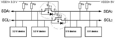
Figure 1. Bi-directional level-shifter circuit connects two different voltage sections of an I2C-bus system. Depending on the MOSFET parameters, the level-shifter can cover a wide range of supply voltages - from as low as 2 V and higher than 5 V if desired. The values of pull-up resistors (and possible series resistors between I/O pins and bus lines) depend on worst case values of the supply voltages and logic levels, the length and load of the bus lines, and rise and fall time requirements. These have to be calculated for each bus system separately. Their values must be chosen in such a way that there is sufficient noise margin at both HIGH and LOW levels. This approach not only provides a level-shifting function for the I2C-bus for all voltage and logic levels, it also provides two additional functions. First, the 'lower voltage' section can be powered-down, effectively removing it from the bus system and allowing the powered 'higher voltage' section to operate normally. Second, it provides a high level of protection to the 'lower voltage' section against voltage spikes produced at the 'higher voltage' section, as long as the MOSFET itself can withstand these spikes. By simply adding another MOSFET on each bus line (see figure 2), an extended power- down structure is achieved. Additional sections with a higher, lower or similar supply voltage can be added by simply connecting them via additional MOSFETs to the common drain terminals. Each individual section can be isolated from the rest of the bus system when its supply voltage is switched off, while level-shifting between all other sections remains operational. VDD3 and the dotted pull-up resistors, which establish a defined level at the common drain connections, are optional. 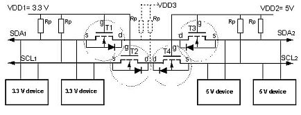
Figure 2. I2C-bus system in which the 'higher voltage' section is isolated at power-off. In addition, the present I2C-bus specification has been extended to cover lower supply voltages and the I2C-bus can now be used for all new devices operating below 2.7 V. Using the low-cost level-shifting solution, these new devices can be kept 100% compatible with devices working at different supply voltages. In fact, in systems relying only on the I2C-bus for inter-IC communication, only two transistors are needed for each separate supply to keep wiring to the absolute minimum (two wires per device). This further enhances the advantage of the I2C-bus over solutions with more signals or random direct connections, because not only is the wiring itself less complex but also substantially fewer level-shifting components are needed. This ensures that I2C-bus applications will continue to expand into the next century.
Philips |
|
Copyright © 2000 Royal Philips Electronics All rights reserved. Terms and conditions. |
|