|
|
|
|
|
|
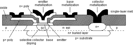
1998-09-21, BG_ic858, Philips Semiconductors' newly announced silicon Monolithic Microwave Integrated Circuits (MMICs) and 5th Generation RF Wideband Transistors, which were launched in February 1997, are both based on a double-poly process - a technology with its roots in integrated circuit production rather than traditional bipolar junction transistor processes. To develop the initial double-polysilicon transistors, the challenge for the team was to adapt the double poly process to the manufacture of high-gain, low-noise, small-signal transistors for use in the front-end receiver sections of 3-volt mobile phones, and high gain, high power-added efficiency (PAE), medium power transistors suitable for use in their RF transmitter sections. Silicon transistors meeting these objectives have a distinct price/performance ratio advantage over competing devices such as GaAs MESFETs. To produce transistors with cut-off frequencies of 25 GHz that will operate at VCE voltages of 3 V or less (all of these transistors still operate at 1 V) it is necessary to achieve base widths in the order of 100 nm. These base widths are achieved by the use of the double-polysilicon process illustrated in figure 1, in which polysilicon (see footnote) is used for both the base and emitter connections. The steep doping profiles of the base and emitter regions create the very narrow base widths required for a high cut-off frequency, while sub-micron emitter widths of typically 0.5 µm (made possible by the self-aligned nature of the process) ensure a high fmax and a low base resistivity. Minimisation of base resistance is essential to achieve the very low noise figures (typically less than 1.2 dB) required in low-noise receiver applications.
Note:
Lateral connection to the base region by p+ polysilicon not only reduces base resistance. Equally as important, it minimises collector-base capacitance and in small-signal types allows single-layer metal (with relaxed design rules) to be used for the emitter and base connections. This construction using single-layer metal is in marked contrast to small-signal double-polysilicon transistors from other manufacturers, which require the use of double-layer metal. Large area metallizations for the emitter allow the transistors to handle the high emitter current densities required in medium-power types. However, producing these 'intrinsic' high-frequency transistors in silicon is only half the story. Their intrinsically high performance can be completely destroyed if the bond-wire and lead-out arrangements in the device package are not carefully designed. In practice it can be shown that bond-wire inductance and collector-base capacitance (CBC ) are the most significant factors that limit the final transistor's high frequency gain. For small-signal types, such as the BFG410W, the dominant contribution to collector-base capacitance comes from the bonding pads rather than from the intrinsic transistor itself. If the transistor die is mounted conventionally, with the substrate forming the collector connection, bond-pad capacitance is unacceptably high. To overcome this problem, Philips Semiconductors fabricates its double-polysilicon transistors using a buried collector layer and then mounts the transistor die 'collector up'. This not only maintains a low value of overall collector-base capacitance, it also minimises the length of the emitter bond-wire and hence reduces emitter inductance. The 'top-side collector' construction of these transistors is illustrated in Figure 2.
For medium-power types designed for use in the RF transmitter sections of mobile phones the critical specifications are power output capability, power gain (GP) and power-added efficiency (PAE). For a given output power, it can be shown that the most important factor in maintaining high power gain is a high IC(max)/CBC ratio. As described earlier, the self-aligned double-polysilicon process already achieves low CBC values, while a high IC(max) specification can be achieved by increasing the collector doping levels. The sub-micron emitter width prevents current crowding effects and helps to keep base resistance low, which in these medium power types is necessary to prevent degradation of power gain. In addition, conduction of heat via the emitter lead frame directly into the pc board provides optimal heatsinking conditions. Operating at 1.8 GHz from a 3.5 V supply, power gains greater than 11 dB and power added efficiencies as high as 60% can be demonstrated.
Silicon MMICs - making 'simple' transistors 'smart' These MMICs have temperature compensation circuitry, biaising and process spread compensation on-chip and are termed 'smart' by Philips Semiconductors because they automatically compensate for process and temperature variations. Despite increasing the complexity of these devices the overall die size is minute, so in many cases the same pacakging can be used for the MMIC as for the single transistor. Several MMICs have been developed (for further technical specification of these devices, please refer to accompanying press release 'Double Poly advance simplifies mobile communications design'):
The Discrete Semiconductors Business Group of Philips Semiconductors is the fourth largest supplier of discrete semiconductors in the world, with an annual turnover in excess of US$ 1 billion. The group's three main areas of expertise are: RF products for mobile communications, video amplifiers for monitors, and RF products for use in infrastructure such as basestations and CATV; power semiconductors for automotive, industrial, lighting and EDP applications; and commodity semiconductors with a broad range of diodes and transistors. This broad product range makes the Discrete Semiconductors Business Group a global supplier to all major segments of the electronics industry. Sales offices are located in all major markets around the world and are supported by systems labs. |
|
Copyright © 2000 Royal Philips Electronics All rights reserved. Terms and conditions. |
|