|
|
|
|
|
1997-07-07
,
E/IC-804/451
Philips Semiconductors has announced that it has developed an ultra fast One Time Programmable (OTP) memory process that is now available in its XA 16 bit and 80C51 8 bit microcontrollers. This process to create EPROM (Electrically Programmable Read Only Memory) results in access times of less than 60 nanoseconds. It was specially developed for Philips Semiconductors by the Philips Research Labs to be closely integrated with Philips' 0.5µ CMOS process, requiring only two more mask steps making it relatively inexpensive to implement. Each memory cell measures only seven square micrometers, giving a high packing density, and can operate between 1.8 and 3.3 V. Memory blocks of up to 4MB in size can be created at a time. The key advantage to customers of OTP memory is that software can be easily loaded into ICs by the customers themselves. Thus code can be quickly tested and improved by simply loading new versions of the code into the ICs rather than having to get a mask change at the manufacturing stage of the ICs. This results in fast software development, fast time to market and the ability to upgrade software easily. In addition, rather than having to stock variants of an IC each with different ROM codes, customers just stock one master IC and then load the appropriate ROM software according to requirements. The initial uses are for consumer communications applications such as cordless telephones and pagers. Capacitors can be easily added Patented way to avoid expensive high voltage transistors Patented overcoat enables Salicide to be laid down for fast operation
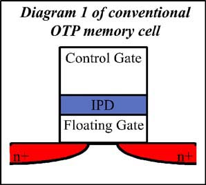
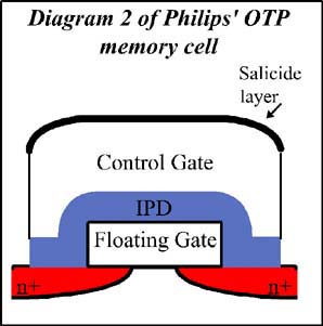
Any attempt to put a layer of Titanium Salicide (TiSi2), or Salicide (Self Aligned Silicide) for short, on the top of the control gate runs into problems with the Salicide going down the sides of the structure and causing shorting between the gates. In the Philips' patented memory cell shown in diagram 2, the control gate overlaps the floating gate completely and so a Salicide layer can be laid down on top with no possibility of shorting occurring. This Salicide layer provides much improved conductivity to the gate, resulting in extremely fast memory access time of less than 60 nanoseconds that Philips believes to be the fastest currently available.
Programming an OTP memory cell The cells are read by applying a small voltage on the control gate to induce conduction in the channel between the source and the drain. But, if the floating gate has a charge, this charge prevents the control gate from inducting conduction in the channel between the source and the drain and so no current flows. By convention, an unaltered cell that allows current to pass equates to a "1" while a programmed non-conducting cell equates to "0". Philips Semiconductors, a division of Philips Electronics NV, headquartered in Eindhoven, The Netherlands, is the ninth largest semiconductor supplier in the world. Philips Semiconductors' innovations in digital audio, video, and mobile technology position the company as a leader in the consumer, multimedia and wireless communications markets. Sales offices are located in all major markets around the world and are supported by regional customer application labs. |
|||||||||||||||||||||||||||||||||||||||||||||||||||||||||||||||
|
Copyright © 2000 Royal Philips Electronics All rights reserved. Terms and conditions. |
|